Publications
Highlights from HEROIC publications
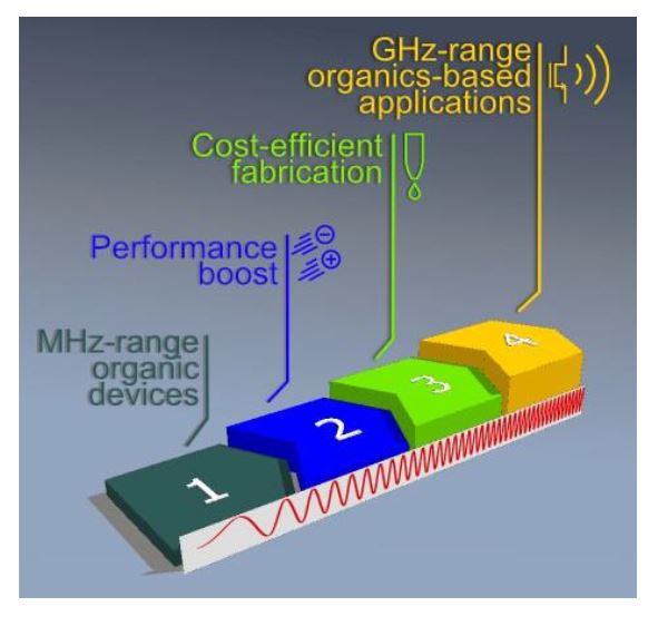
Walking the Route to GHz Solution‐Processed Organic Electronics: A HEROIC Exploration
Andrea Perinot, Bianca Passarella, Michele Giorgio, Mario Caironi
Limited charge carrier mobility of organic semiconductors, especially for solution‐processed polymer thin films, has typically relegated organic electronics to low‐frequency operation. Nevertheless, thanks to a steady increase in electronic properties of organics, much higher operation frequencies are feasible, suggesting a possible and appealing scenario where lightweight, cost‐effective, and conformable electronics can integrate both sensing and radio‐frequency transmitting functionalities, which are the key to unlock pervasive networks of distributed sensors revolutionizing human–environment interaction. Few years ago, it was suggested that gigahertz (GHz) field‐effect transistors could be achievable even with solution‐based processes. This was the basis for the European Research Council project high‐frequency printed and direct‐written organic‐hybrid integrated circuits (HEROIC), which in the last few years investigated such unexplored path. Here, the authors report their vision toward the achievement of radio‐frequency organic electronics mainly with solution‐based and scalable processes, with reference to the experience of the HEROIC project and to some of the most notable literature examples. The authors show that the achievement of solution‐processable organic field‐effect transistors with GHz operation is indeed feasible, but requires considering a carefully revised scenario in which the main role is played by charge injection, together with the geometric overlap, the capacitive parasitism associated to fringing and some constraints on the dielectric layer thickness.
Radio-Frequency Polymer Field-Effect Transistors Characterized by S-Parameters
Michele Giorgio, Mario Caironi
Thanks to recent progress in terms of materials properties, polymer field-effect transistors (FETs) operating in the MHz range can be achieved. However, further development toward challenging frequency ranges, for a field accustomed to slow electronic devices, has to be addressed with suitable device design and measurements methodologies. In this letter, we report n-type FETs based on a solution-processed polymer semiconductor where the critical features have been realized by a large-area compatible direct-writing technique, allowing to obtain a maximum frequency of transition of 19 MHz, asmeasured bymeans of ScatteringParameters(S-Parameters). This is the first report of solution-processed organic FETs characterized with SParameters
Accessing MHz Operation at 2 V with Field‐Effect Transistors Based on Printed Polymers on Plastic
Andrea Perinot, Mario Caironi
Organic printed electronics are suitable for the development of wearable, lightweight, distributed applications in combination with cost‐effective production processes. Nonetheless, some necessary features for several envisioned disruptive mass‐produced products are still lacking: among these radio‐frequency (RF) communication capability, which requires high operational speed combined with low supply voltage in electronic devices processed on cheap plastic foils. Here, it is demonstrated that high‐frequency, low‐voltage, polymer field‐effect transistors can be fabricated on plastic with the sole use of a combination of scalable printing and digital laser‐based techniques. These devices reach an operational frequency in excess of 1 MHz at the challengingly low bias voltage of 2 V, and exceed 14 MHz operation at 7 V. In addition, when integrated into a rectifying circuit, they can provide a DC voltage at an input frequency of 13.56 MHz, opening the way for the implementation of RF devices and tags with cost‐effective production processes.
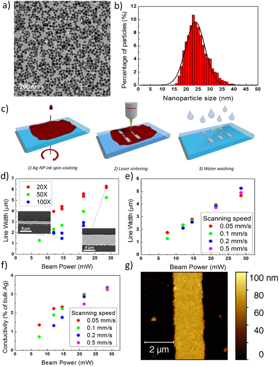
Direct-written polymer field-effect transistors operating at 20 MHz
Andrea Perinot, Prakash Kshirsagar, Maria Ada Malvindi, Pier Paolo Pompa, Roberto Fiammengo and Mario Caironi
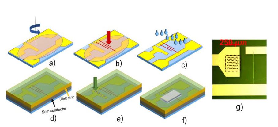
Printed polymer electronics has held for long the promise of revolutionizing technology by delivering distributed, flexible, lightweight and cost-effective applications for wearables, healthcare, diagnostic, automation and portable devices. While impressive progresses have been registered in terms of organic semiconductors mobility, field-effect transistors (FETs), the basic building block of any circuit, are still showing limited speed of operation, thus limiting their real applicability. So far, attempts with organic FETs to achieve the tens of MHz regime, a threshold for many applications comprising the driving of high resolution displays, have relied on the adoption of sophisticated lithographic techniques and/or complex architectures, undermining the whole concept. In this work we demonstrate polymer FETs which can operate up to 20 MHz and are fabricated by means only of scalable printing techniques and direct-writing methods with a completely mask-less procedure. This is achieved by combining a fs-laser process for the sintering of high resolution metal electrodes, thus easily achieving micron-scale channels with reduced parasitism down to 0.19 pF mm−1, and a large area coating technique of a high mobility polymer semiconductor, according to a simple and scalable process flow.

Macroscopic and high-throughput printing of aligned nanostructured polymer semiconductors for MHz large-area electronics
Sadir G. Bucella, Alessandro Luzio, Eliot Gann, Lars Thomsen, Christopher R. McNeill, Giuseppina Pace, Andrea Perinot, Zhihua Chen, Antonio Facchetti and Mario Caironi
High-mobility semiconducting polymers offer the opportunity to develop flexible and large-area electronics for several applications, including wearable, portable and distributed sensors, monitoring and actuating devices. An enabler of this technology is a scalable printing process achieving uniform electrical performances over large area. As opposed to the deposition of highly crystalline films, orientational alignment of polymer chains, albeit commonly achieved by non-scalable/slow bulk alignment schemes, is a more robust approach towards large-area electronics. By combining pre-aggregating solvents for formulating the semiconductor and by adopting a room temperature wired bar-coating technique, here we demonstrate the fast deposition of submonolayers and nanostructured films of a model electron-transporting polymer. Our approach enables directional self-assembling of polymer chains exhibiting large transport anisotropy and a mobility up to 6.4 cm2 V−1 s−1, allowing very simple device architectures to operate at 3.3 MHz. Thus, the proposed deposition strategy is exceptionally promising for mass manufacturing of high-performance polymer circuits.
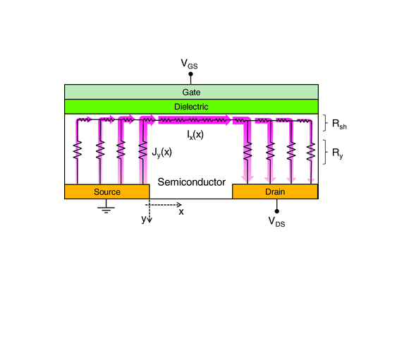
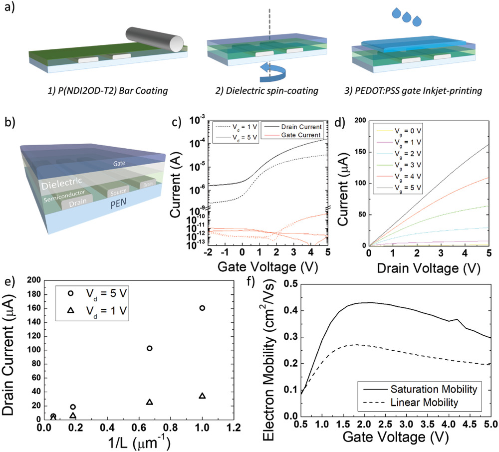
Injection Length in Staggered Organic Thin Film Transistors: Assessment and Implications for Device Downscaling
Dario Natali, Jiaren Chen, Francesco Maddalena, Francisco García Ferré, Fabio Di Fonzo and Mario Caironi
In staggered thin film transistors, the injection length is the fraction of the gate to contact overlap that is effectively involved in current injection. Its assessment is important to properly downscale device dimensions. In fact, in order to increase transistor operation speed, the whole device footprint should be downscaled, which means both the gate to contact overlap and the channel length, as they affect the relative weight of gate to contact parasitic capacitances and the carrier transit time along the channel respectively. Nevertheless, it is not advisable to make the gate to contact overlap smaller than the injection length, because this negatively affects contact resist- ances. Suitable figures of merits are introduced to quantify these aspects, and a method is proposed to extract the injection length from electrical measurements. As an example of application, transistors based on the prototypical n-type polymer poly{[N,N′-bis(2-octyldodecyl)-naphthalene- 1,4,5,8-bis(dicarboximide)-2,6-diyl]-alt-5,5′-(2,2′-bithiophene)} (P(NDI2OD- T2) are analyzed. When the channel length is scaled while driving voltages are kept constant, in P(NDI2OD-T2) the injection length decreases as well, thus proving that the downscaling of the whole device footprint is feasible. The physical origins of this finding are analyzed and traced back to material properties, in order to suggest general guidelines for a successful transistor downscaling.
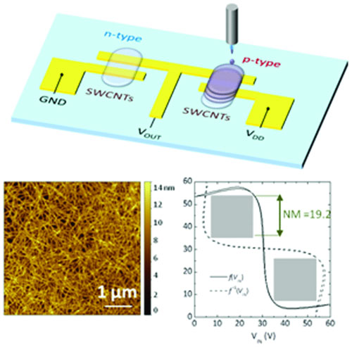
Inkjet Printed Single-Walled Carbon Nanotube Based Ambipolar and Unipolar Transistors for High-Performance Complementary Logic Circuits
Sadir Gabriele Bucella, Jorge Mario Salazar-Rios, Vladimir Derenskyi, Martin Fritsch, Ullrich Scherf, Maria Antonietta Loi, and Mario Caironi
Inkjet printed single walled carbon nanotubes (SWCNT) field-effect transistors with mobilities of 15 and 7 cm2 V−1 s−1for holes and electrons, respectively, and high on–off ratio, are demonstrated. The high loading of the ink formulation and high electronic quality of the sorted SWCNT enable facile printing of networks displaying high coverage and effective mobility already after a single printing pass. Balanced ambipolarity or mainly unipolar behavior can be tuned by simply varying the number of printing passes, thus enabling the realization of high-performance complementary-like logic gates.
High-Mobility Naphthalene Diimide and Selenophene-Vinylene-Selenophene-Based Conjugated Polymer: n-Channel Organic Field-Effect Transistors and Structure–Property Relationship
Min Jae Sung, Alessandro Luzio, Won-Tae Park, Ran Kim, Eliot Gann,Francesco Maddalena, Giuseppina Pace, Yong Xu, Dario Natali, Carlo de Falco, Long Dang, Christopher R. McNeill, Mario Caironi, Yong-Young Noh, and Yun-Hi Kim
Interdependence of chemical structure, thin-film morphology, and transport properties is a key, yet often elusive aspect characterizing the design and development of high-mobility, solution-processed polymers for large-area and flexible electronics applications. There is a specific need to achieve >1 cm2 V−1 s−1 field-effect mobilities (μ) at low processing temperatures in combination with environmental stability, especially in the case of electron-transporting polymers, which are still lagging behind hole transporting materials. Here, the synthesis of a naphthalene-diimide based donor–acceptor copolymer characterized by a selenophene vinylene selenophene donor moiety is reported. Optimized field-effect transistors show maximum μ of 2.4 cm2 V−1 s−1 and promising ambient stability. A very marked film structural evolution is revealed with increasing annealing temperature, with evidence of a remarkable 3D crystallinity above 180 °C. Conversely, transport properties are found to be substantially optimized at 150 °C, with limited gain at higher temperature. This discrepancy is rationalized by the presence of a surface-segregated prevalently edge-on packed polymer phase, dominating the device accumulated channel. This study therefore serves the purpose of presenting a promising, high-electron-mobility copolymer that is processable at relatively low temperatures, and of clearly highlighting the necessity of specifically investigating channel morphology in assessing the structure–property nexus in semiconducting polymer thin films.
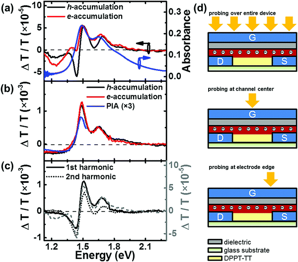
Ambipolar charge distribution in donor–acceptor polymer field-effect transistors
Xin Yu Chin, Giuseppina Pace, Cesare Soci and Mario Caironi
Recent developments in the design and synthesis of donor–acceptor semiconducting copolymers have significantly contributed to improve the ambipolar transport properties of polymer field-effect transistors (FETs). The further development of such FETs towards real applications would greatly benefit from the knowledge of the specific charge distribution along the channel, especially in the ambipolar regime. Here we accomplish this task by adopting charge modulation spectroscopy (CMS) and microscopy (CMM), electro-optical spectroscopy techniques which allow us to probe in situ charge induced features in the transmission spectra of conjugated polymers, to study a model high mobility donor–acceptor co-polymer (DPPT-TT, poly(N-alkyldiketopyrrolo-pyrrole dithienylthieno[3,2-b]thiophene)). Thanks to the sub-micrometer spatial resolution of confocal microscopy, we are able to isolate the specific contribution of channel and electrode regions which are superimposed in the macroscopic CMS spectra, thus allowing the mapping of hole and electron distributions across the active channel in both unipolar and ambipolar operating regimes. Our findings illustrate the use of a local probe in charge-modulation experiments to correctly assign spectral features and to determine the distributions of positive and negative charge carriers in an operating device, which has relevant implications on the understanding of the nature of charge transport in high-mobility ambipolar semiconducting polymers.
Full publications list with HEROIC contribution
S. Schmidt, M. Hoenig, Y. Shin, M. Cassinelli, A. Perinot, M. Caironi, X. Jiao, C. R. McNeill, D. Fazzi, T. Biskup, and M. Sommer
ACS Applied Polymer Materials, 2, 5, 1954–1963, 2020
DOI: https://doi.org/10.1021/acsapm.0c00151
Probing Mobile Charge Carriers in Semiconducting Carbon Nanotube Networks by Charge Modulation Spectroscopy
N. F. Zorn, F. Scuratti, F. J. Berger, A. Perinot, D. Heimfarth, M. Caironi, and J. Zaumseil
ACS Nano 14, 2, 2412-2423, 2020
DOI: https://doi.org/10.1021/acsnano.9b09761
Walking the Route to GHz Solution‐Processed Organic Electronics: An HEROIC Exploration
A. Perinot, B. Passarella, M. Giorgio, and M. Caironi
Adv. Funct. Mater. 1907641, 2020
DOI: https://doi.org/10.1002/adfm.201907641
Flexible low-voltage organic thin-film transistors with low contact resistance and high transit frequencies
J. W. Borchert, U. Zschieschang, F. Letzkus, M. Giorgio, M. Caironi, J. N. Burghartz, S. Ludwigs, and H. Klauk
26th International Workshop on Active-Matrix Flatpanel Displays and Devices (AM-FPD), 2019
DOI: 10.23919/AM-FPD.2019.8830580
Radio-Frequency Polymer Field-Effect Transistors Characterized by S-Parameters
M. Giorgio, and M. Caironi
IEEE Electron Device Letters 40 (6), 953-956, 2019
Accessing MHz Operation at 2 V with Field‐Effect Transistors Based on Printed Polymers on Plastic
A.Perinot, and M. Caironi
Advanced Science 6 (4), 1801566, 2019
DOI: https://doi.org/10.1002/advs.201801566
Roadmap to Gigahertz Organic Transistors
U. Zschieschang, J. W. Borchert, M. Giorgio, M. Caironi, F. Letzkus, J. N. Burghartz, U. Waizmann, J. Weis, S. Ludwigs, and H. Klauk
Advanced Functional Materials, 1903812, 2019
DOI: https://doi.org/10.1002/adfm.201903812
Development of organic field-effect transistors for operation at high frequency
Flexible Carbon-based Electronics, 71-94, 2018
A Defect-Free Naphthalene Diimide Bithiazole Copolymer via Regioselective Direct Arylation Polycondensation
Record Static and Dynamic Performance of Flexible Organic Thin-Film Transistors
Low‐Voltage, Printed, All‐Polymer Integrated Circuits Employing a Low‐Leakage and High‐Yield Polymer Dielectric
Thermoelectrics: From history, a window to the future
Ultraconformable Freestanding Capacitors Based on Ultrathin Polyvinyl Formal Films
Tattoo-Like Transferable Hole Selective Electrodes for Highly Efficient, Solution-Processed Organic Indoor Photovoltaics
Reproducible, High Performance Fully Printed Photodiodes on Flexible Substrates through the Use of a Polyethylenimine Interlayer
Experimental investigation of the mechanical robustness of a commercial module and membrane-printed functional layers for flexible organic solar cells
Drastic Improvement of Air Stability in an n-Type Doped Naphthalene-Diimide Polymer by Thionation
N -Alkyl substituted 1 H -benzimidazoles as improved n-type dopants for a naphthalene-diimide based copolymer
Diffractive X-ray Waveguiding Reveals Orthogonal Crystalline Stratification in Conjugated Polymer Thin Films
Tattoo-Paper Transfer as a Versatile Platform for All-Printed Organic Edible Electronics
Contact potential and scanning Kelvin force microscopy measurements on sulphate-anion intercalated graphite
Controlling the Functional Properties of Oligothiophene Crystalline Nano/Microfibers via Tailoring of the Self-Assembling Molecular Precursors
Improving Miscibility of a Naphthalene Diimide-Bithiophene Copolymer with n-Type Dopants through the Incorporation of ‘Kinked’ Monomers
Transparent and Highly Responsive Phototransistors Based on a Solution-Processed, Nanometers-Thick Active Layer, Embedding a High-Mobility Electron-Transporting Polymer and a Hole-Trapping Molecule
Transparent and Highly Responsive Phototransistors Based on a Solution-Processed, Nanometers-Thick Active Layer, Embedding a High-Mobility Electron-Transporting Polymer and a Hole-Trapping Molecule
Ultrahigh Mobility in Solution-Processed Solid-State Electrolyte-Gated Transistors
Highly Planarized Naphthalene Diimide–Bifuran Copolymers with Unexpected Charge Transport Performance
Water-Gated n‑Type Organic Field-Effect Transistors for Complementary Integrated Circuits Operating in an Aqueous Environment
On the Effect of Prevalent Carbazole Homocoupling Defects on the Photovoltaic Performance of PCDTBT:PC71BM Solar Cells
Self-aligned organic field-effect transistors on plastic with picofarad overlap capacitances and megahertz operating frequencies
Complementary Organic Logic Gates on Plastic Formed by Self-Aligned Transistors with Gravure and Inkjet Printed Dielectric and Semiconductors
Stuart G. Higgins, Beinn V. O. Muir, Giorgio Dell'Erba, Andrea Perinot, Mario Caironi andAlasdair J. Campbell
Adv. Electron. Mater., 2, 2, 2016
Two-dimensional charge transport in molecularly ordered polymer field-effect transistors
Effects of PNDIT2 end groups on aggregation, thin film structure, alignment and electron transport in field-effect transistors
High-Performance Organic Field-Effect Transistors with Directionally Aligned Conjugated Polymer Film Deposited from Pre-Aggregated Solution