Objectives and Plan


-
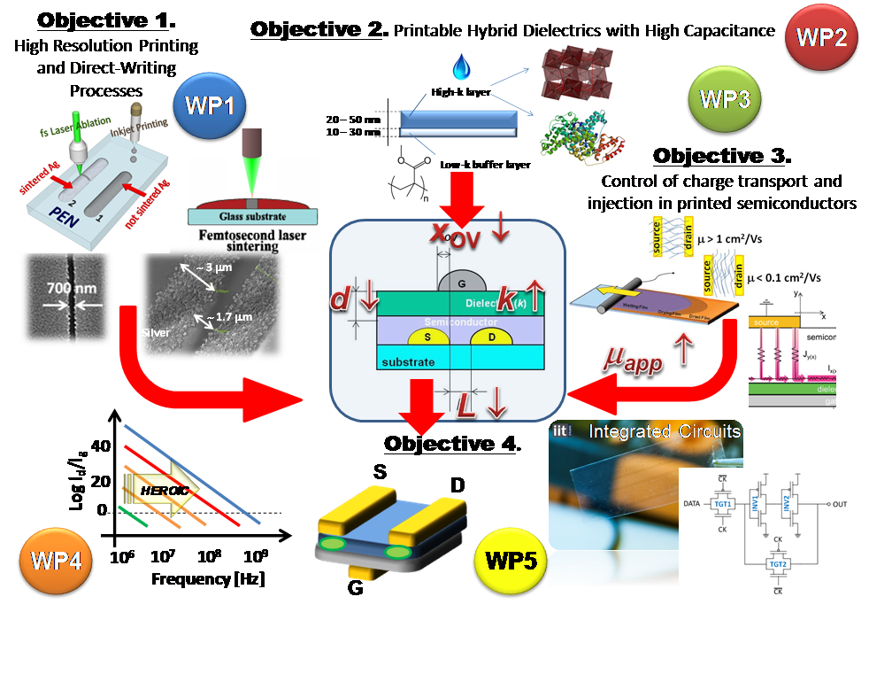
Development of scalable high resolution printing and direct-writing processes for the patterning of functional inks on flexible substrates
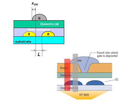
 Target materials will be primarily conductors, to be patterned on plastic, since high resolution is a mandatory requisition especially for the patterning of devices electrodes. The goal is to proceed far beyond the state-of-the-art in both achievable channel lengths and linewidths. In the former case the goal is to develop scalable, maskless processes to achieve L < 2 µm, with a final aim below 1 µm; in the latter case, linewidths of only a few microns, with a final goal around 1 µm, are the target.
 -
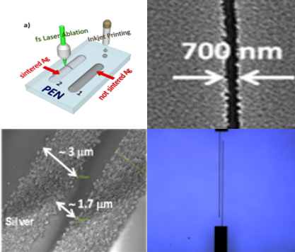
Development of printable hybrid dielectrics with high specific capacitances
 At the starting of HEROIC project, the scarce examples of all-printed organic transistors or circuits showed polymeric dielectrics hundreds of nanometers thick at least, with capacitances < 5 nF/cm2, completely unsuitable for downscaled, low-voltage FETs. HEROIC will develop printable low leakage nano-scale dielectrics based on a stack of solution-processable organic and inorganic materials in a hybrid approach. The target specific capacitance is set in the 100-200 nF/cm2 range, as this is sufficient to correctly drive a downscaled device in the 1 to 5 V range, suitable for real applications. Developing printable dielectrics that can be easily integrated into a wide range of architectures is an important goal to allow the development of novel high-frequency layouts.
 -
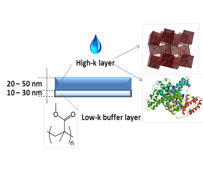
Advanced control of charge injection and transport in printed polymer and hybrid semiconductors
 One of the main breakthroughs will be the alignment of polymers films, and the control of long-range orientational order and anisotropy, with simple coating/printing techniques as a way to improve charge transport properties and reduce scattering of device parameters. Solution-based doping protocols will be explored in order to optimize charge injection in advanced device layouts. In parallel, hybrid approaches will be developed, where the optimal mechanical properties of polymers and ease of processability of polymer based inks, for flexible and large-area electronics, are combined with the inclusion of other semiconductors characterized by coherent transport, in order to improve charge transport.
 -
Final Goal. Development of flexible, polymer and hybrid transistors with fT = 1 GHz fabricated only by means of scalable printing and direct-writing techniques, and their integration into fast printed circuits
 The goal is to improve by more than 3 orders of magnitude what could be found in the literature at the starting of the HEROIC project with solution-based processes, therefore setting new paradigms for fast printed electronics preserving manufacturability over large areas on flexible foils. Further part of this objective is to integrate both p and n channel devices in fast-switching integrated plastic circuits. The consequent target is the achievement of clock rates in the 10 to 100 MHz range (i.e. a 5 stage ring oscillator with stage delay from 1 to 10 ns).
 -
Overall